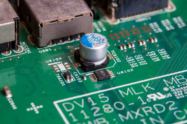
In modern electronics, electrolytic capacitors play a crucial role in power management, noise filtering, and signal stabilization. Among them, the 16V 1000uF SMD 4 x 5.4mm electrolytic capacitor is widely used due to its compact size and reliable performance. If you’re a PCB designer using KiCad, understanding how to properly integrate this component into your project is essential. This article will walk you through everything you need to know about the 16V 1000uF SMD 4 x 5.4mm electrolytic capacitor KiCad model, from technical specifications and footprint creation to 3D modeling and usage tips.
Understanding the 16V 1000uF SMD Electrolytic Capacitor
Electrolytic capacitors are polarized capacitors designed to store large amounts of energy. The 16V 1000uF variant specifically refers to:
- Voltage Rating: 16 volts, the maximum voltage the capacitor can safely handle.
- Capacitance: 1000 microfarads (uF), indicating how much charge it can store.
- Package Type: Surface Mount Device (SMD), making it suitable for automated assembly processes.
- Dimensions: 4 x 5.4mm, denoting the diameter and height, which is important for footprint design and clearance.
This capacitor is ideal for use in low-voltage DC power supplies, voltage regulation circuits, and smoothing applications in compact PCBs.
Why Accurate Modeling in KiCad Matters
In PCB design, modeling your components accurately in your EDA tool like KiCad ensures:
- Proper physical placement and layout.
- Accurate 3D rendering for enclosure design.
- Reliable BOM (Bill of Materials) generation.
- Reduced manufacturing errors.
The 16V 1000uF SMD 4 x 5.4mm electrolytic capacitor KiCad model is not always available in the default KiCad libraries. You may need to create or import a custom footprint and 3D model.
Creating the KiCad Symbol for the Capacitor
- Open KiCad’s Symbol Editor.
- Create a New Symbol: Choose a category (e.g., “Capacitors”) and click “New Symbol”.
- Name the Symbol: Something identifiable like C_Elec_SMD_1000uF_16V_4x5.4.
- Draw the Symbol:
- Use the standard polarized capacitor symbol.
- Label the pins as “+” and “-”.
- Assign appropriate properties (capacitance, voltage rating, etc.).
- Add Symbol Fields:
- Value: 1000uF
- Footprint: Will be linked later
- Datasheet: Add a reference to the component’s datasheet if available
Designing the KiCad Footprint
- Open KiCad Footprint Editor.
- Create a New Footprint: Name it CP_Elec_SMD_4x5.4mm_Pad1.4mm.
- Define Pads:
- Create two rectangular or oval pads spaced according to the manufacturer’s specification (typically 2mm–3mm apart).
- Recommended pad size: ~1.4mm diameter.
- Outline the Body:
- Use silkscreen to draw the capacitor’s circular outline.
- Indicate the polarity with a clear “+” sign near the positive pad.
- Add Courtyard and Fab Layers:
- Define physical dimensions for design rule checking and manufacturing.
Adding a 3D Model (Optional but Recommended)
To visualize your design in 3D:
- Find or Create a 3D Model:
- You can search on sites like 3DContentCentral or create one using FreeCAD.
- Save the file in .wrl (VRML) or .step format.
- Link 3D Model to Footprint:
- In Footprint Editor, go to “3D Settings”.
- Add the path to your 3D model file.
- Adjust position, scale, and rotation to match the physical specs.
How to Use the Capacitor in a KiCad Project
Once you’ve created the symbol and footprint:
- Add the Symbol to Schematic:
- Open your schematic and place the capacitor symbol.
- Connect it according to your circuit design.
- Assign the Footprint:
- Either directly from the symbol editor or through the CvPCB tool.
- Annotate and Validate:
- Use the “Annotate Schematic” tool.
- Run ERC (Electrical Rule Check) to verify connections.
- Update PCB Layout:
- Import the netlist into the PCB Editor.
- Place the capacitor and route its connections.
- Run DRC and View 3D Model:
- Use the Design Rule Check to catch spacing or clearance issues.
- Use the 3D viewer to ensure physical compatibility with your design.
Tips for SMD Electrolytic Capacitor Placement
- Polarity Matters: Ensure the orientation matches the schematic. Incorrect placement can damage the circuit.
- Keep Away from Heat: Electrolytic capacitors degrade faster when exposed to high temperatures. Place them away from high-power components.
- Use Thermal Reliefs: If connected to a ground plane, use thermal relief to simplify soldering.
Example Applications
- DC-DC Converters: Smoothing output ripple in buck/boost regulators.
- Audio Circuits: Power filtering in preamp stages.
- Microcontroller Boards: Voltage stabilization near Vcc pins.
- IoT Devices: Compact size is suitable for battery-powered designs.
Common Mistakes to Avoid
- Wrong Footprint Dimensions: Always check the datasheet before creating or selecting a footprint.
- No Courtyard Clearance: Not defining proper courtyard can cause issues during automated assembly.
- Polarity Errors in Layout: Always double-check the orientation using silkscreen markings and schematic labels.
Final Thoughts
The 16V 1000uF SMD 4 x 5.4mm electrolytic capacitor KiCad model may seem like a minor detail in a large PCB project, but its correct implementation ensures reliability and performance. Creating a custom symbol and footprint might take a little time upfront, but it pays off in smoother designs and fewer manufacturing issues. Whether you’re designing power management systems, audio boards, or compact IoT devices, this capacitor’s size and capacity make it a go-to component.
By mastering how to accurately model and integrate such components in KiCad, you level up your PCB design skills and build more professional and production-ready circuits.


